Toward Self-Sufficiency: China’s Equipment Development Strategy
Toward Self-Sufficiency: China’s Equipment Development Strategy
- Source: SemiVision
- Author: SEMIVISION
- Published: 2025-03-26T23:56:30+08:00
- URL: https://tspasemiconductor.substack.com/p/toward-self-sufficiency-chinas-equipment (1) Toward Self-Sufficiency: China’s Equipment Development Strategy


Toward Self-Sufficiency: China’s Equipment Development Strategy
Original Article by SemiVision Research

Mar 26, 2025
∙ Paid
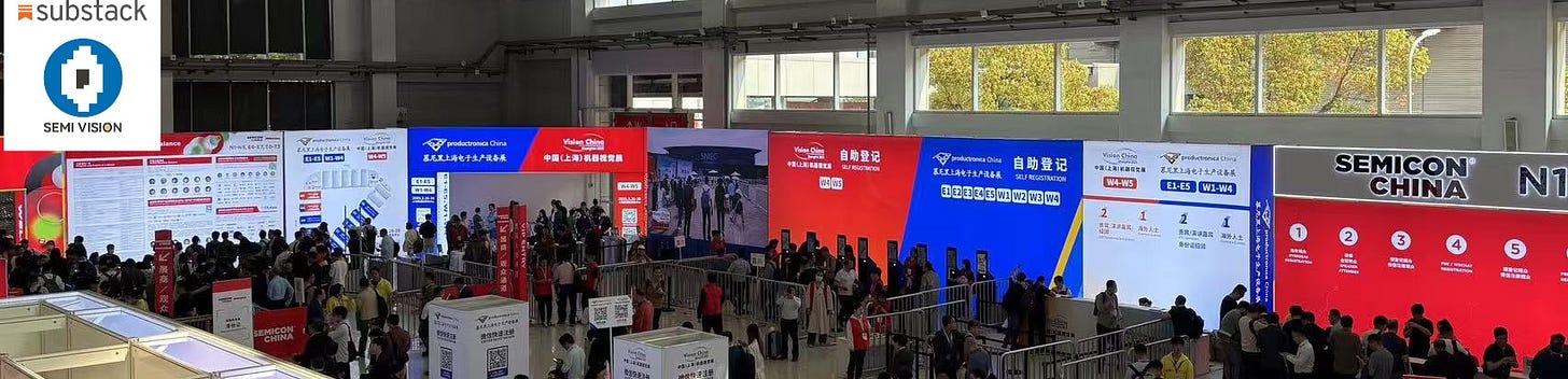
SEMICON China Launches: Chinese Semiconductor Equipment Players Showcase Emerging Technologies
SemiVisionResearch shares noteworthy developments from the floor

Huawei’s 5nm Hope?
Mysterious Provider— Chip Equipment Firm to Unveil “阿里山 (Alishan)”

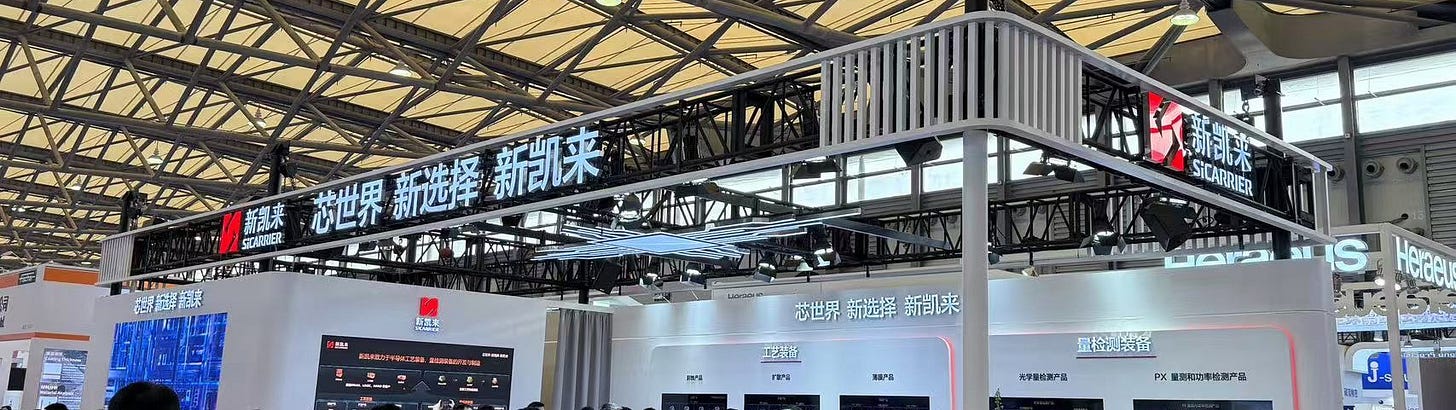
Chinese semiconductor equipment manufacturerSiCarrier (新凱來), which is reported to have close ties with Huawei, is set to debut a range of new products at SEMICON China. Whether the company will present 5nm-compatible equipment has drawn considerable attention.
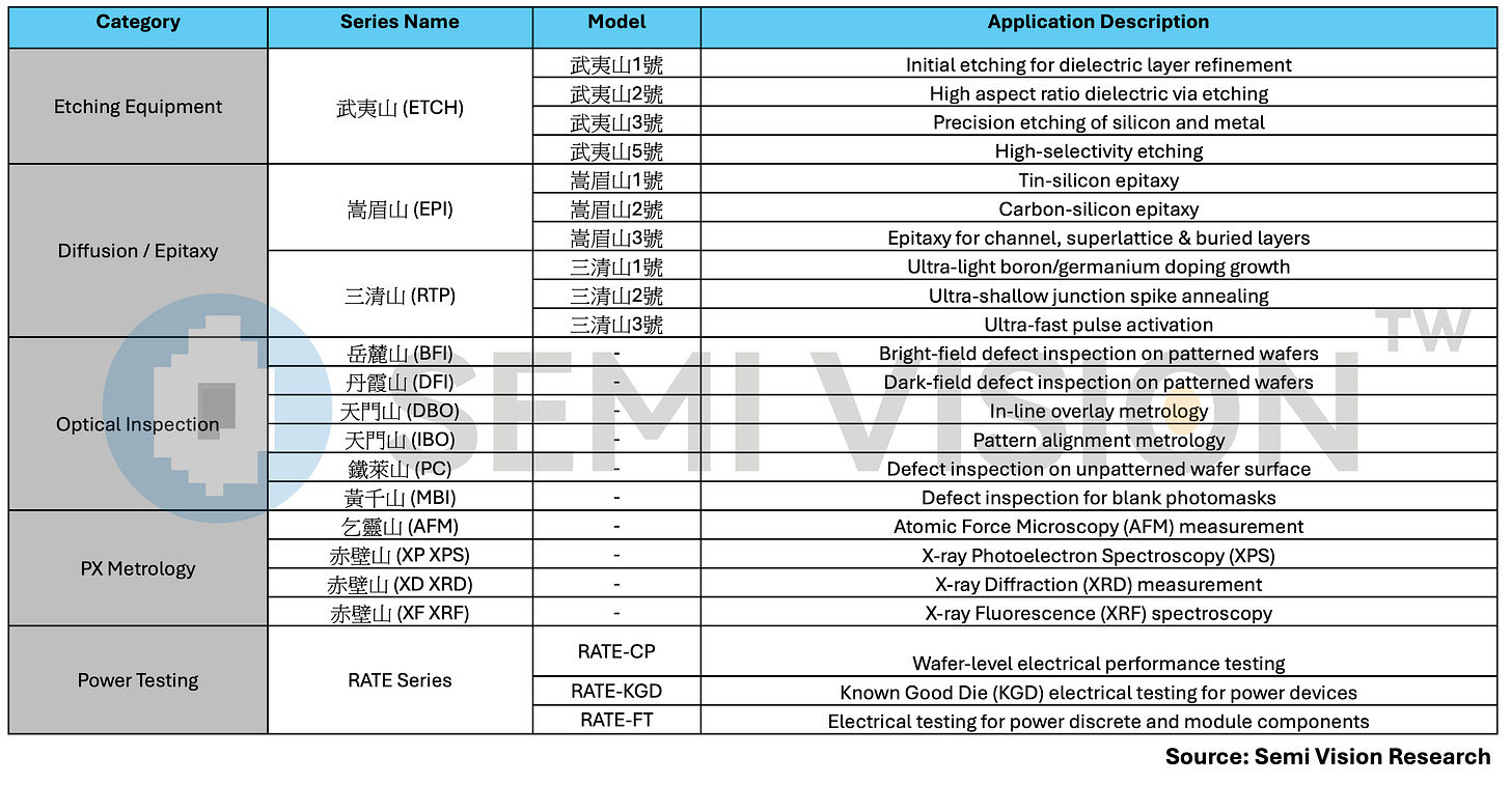
SiCarrier’s new product lineup is uniquely named after famous Chinese mountains, including:

• Epitaxy system “峨眉山 (Emei Mountain)”

• Etching systems “武夷山 (Wuyi Mountain)”

• Chemical Vapor Deposition (CVD) system “長白山 (Changbai Mountain)”

• Atomic Layer Deposition (ALD) tool “阿里山 (Alishan, TW)”

While the company’s patent portfolio has garnered interest, its ability to achieve mass production and integrate a robust supply chain remains an open question. Advanced chip manufacturing requires coordinated breakthroughs across lithography, materials, EDA tools, and other domains.
“China’s development of ALD and related technologies may have ripple effects beyond semiconductors, influencing sectors such as optical coatings and consumer applications,” said a SemiVision Research “This is something Taiwan must watch closely.”
ALD: A Critical Enabler for Advanced Nodes

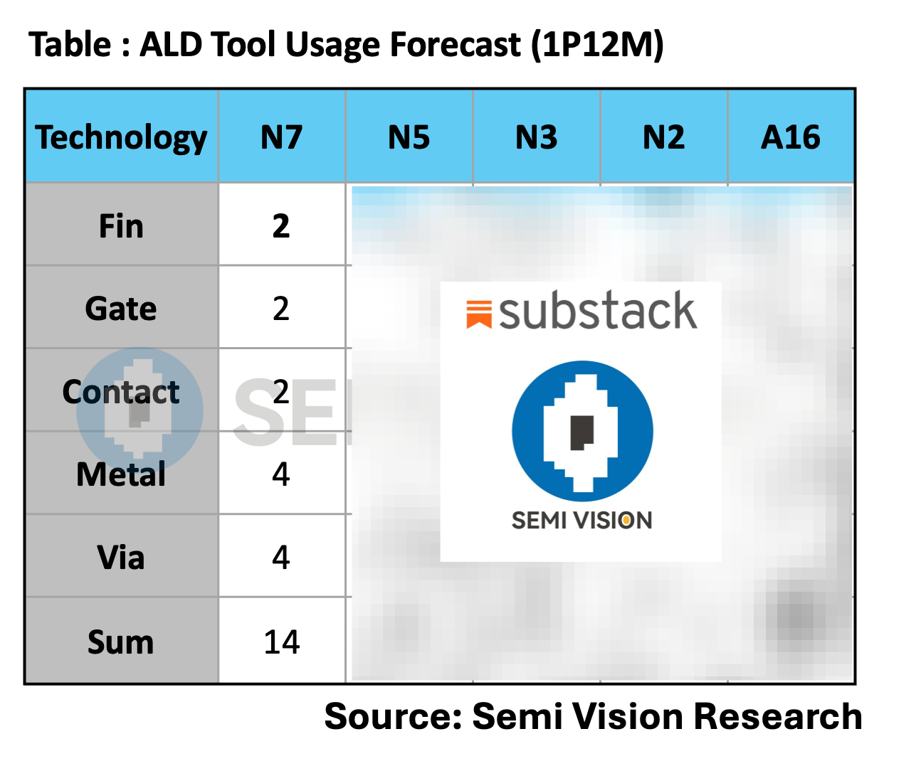
According to SemiVision Research, ALD has become a critical step in advanced semiconductor processes. In thin-film deposition, there are two main categories: oxide layers and metal layers. Traditionally, PVD (Physical Vapor Deposition) has been used for metal deposition. However, as feature sizes shrink and aspect ratios grow, ALD (Atomic Layer Deposition) is increasingly essential due to its atomic-level precision and conformality.

Physical Vapor Deposition (PVD) and Atomic Layer Deposition (ALD) are two of the most critical thin-film deposition techniques in semiconductor manufacturing.
PVD remains a cost-effective, high-throughput option for conventional metal deposition in legacy and mid-range nodes. But as device geometries shrink and 3D architectures proliferate, ALD is indispensable for its uniformity, precision, and compatibility with FinFET, GAA, and heterogeneous integration.
For sub-5nm nodes and future chip architectures, ALD will continue to be favored despite its complexity and higher cost.

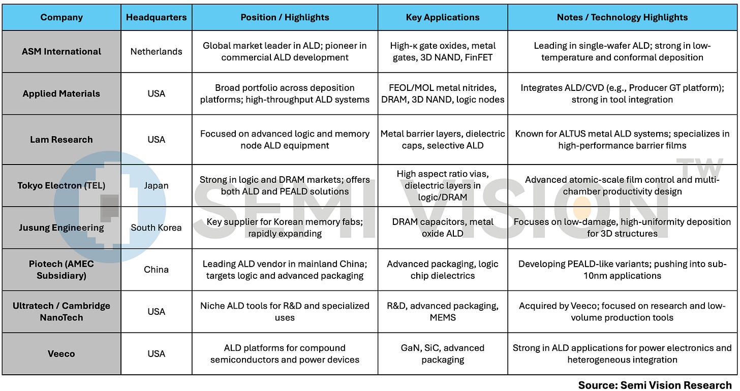
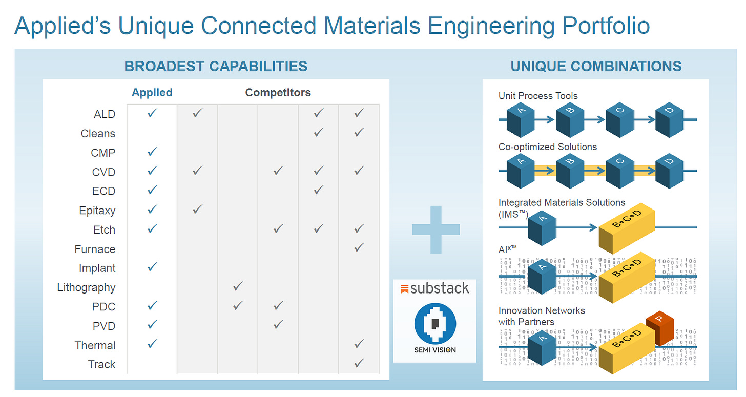
Major Global ALD Equipment Supplier


Huawei Patent on SAQP: Toward DUV-based 5nm Manufacturing?
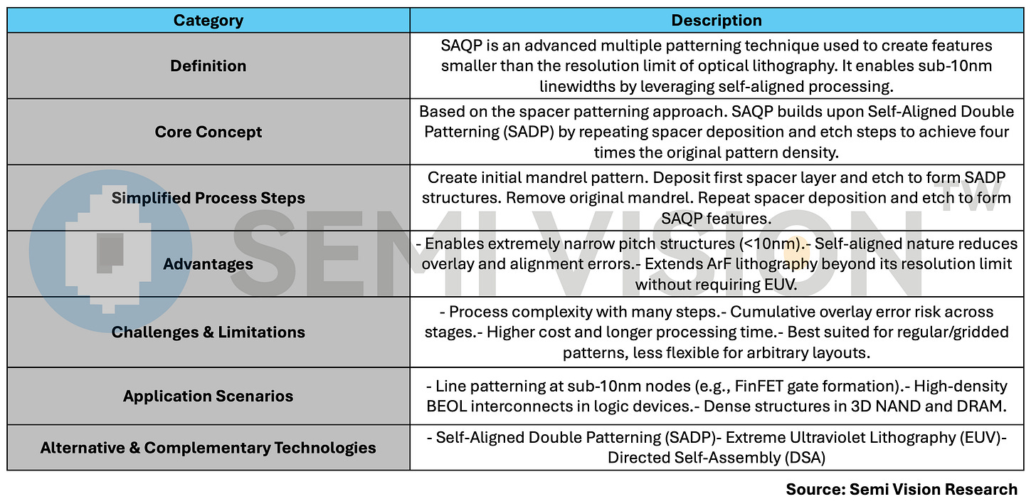
According to the China National Intellectual Property Administration (CNIPA), Huawei Technologies Co., Ltd. filed a patent in September 2021 titled“Method for Manufacturing Semiconductor Device Using Self-Aligned Quadruple Patterning”(Publication No.CN117751427A).

The patent describes a technique leveraging Self-Aligned Quadruple Patterning (SAQP) to etch multiple dense lines on a silicon wafer, thereby increasing transistor density and enhancing chip performance. This method is aimed at enabling 5nm-class chip manufacturing using deep ultraviolet (DUV) lithography, reducing dependence on EUV tools.
The South China Morning Post previously reported that SiCarrier, backed by the Shenzhen municipal government, gained attention in 2023 after acquiring a patent related to 5nm manufacturing using DUV. The company is speculated to be a key technology provider behind Huawei’s Mate 60 Pro smartphone, which launched in 2024 with a 7nm chip despite U.S. export controls.
SiCarrier maintains a low public profile. Its official website only notes that it is a subsidiary of Shenzhen Major Industrial Investment Group, founded in 2021—coinciding with tightened U.S. sanctions on Huawei. The site lists only four entry-level semiconductor tools, with no information on executive leadership or company ownership.
Recently, the company published its first official WeChat article, announcing its participation in SEMICON China and claiming its role as a “core semiconductor equipment supplier” committed to the “development and manufacturing of advanced semiconductor tools.”



For Paid Members, SemiVision Research will discuss following topics:
The Competitive Landscape of Semiconductor Equipment: Global Leaders vs China’s Rise
SiCarrier’s “Mountain Series” Semiconductor Equipment: Strategic Deployment for Advanced Node Manufacturing
Restructuring the Fab Equipment Ecosystem: Global Incumbents vs. China’s Contenders
SiCarrier Core Equipment Highlights
SiCarrier Metrology & Inspection Strategy
SiCarrier Breakthroughs in Metrology & Inspection
The Competitive Landscape of Semiconductor Equipment: Global Leaders vs China’s Rise
As the global semiconductor industry enters the sub-10nm era and rapidly scales advanced packaging and heterogeneous integration, wafer fabrication equipment (WFE) suppliers have become more strategically critical than ever. Global leaders such as ASML, Applied Materials, Lam Research, and Tokyo Electron dominate key segments—from EUV lithography to advanced etch and atomic-scale deposition—with decades of experience, tightly integrated ecosystems, and unmatched field-proven reliability.
In contrast, China’s domestic equipment players, including AMEC, NAURA, ACM Research, and emerging firms likeSiCarrier, have rapidly gained momentum under strong national policy support and the rising urgency of supply chain localization. These companies are making notable progress in ALD, CVD, PVD, RTP, and metrology tools, with some platforms already verified by leading Chinese fabs such as SMIC and YMTC.
Case Example – SiCarrier “Alishan” ALD System
SiCarrier’sAlishan ALD systemhas successfully passed production-line verification at SMIC Shenzhen, supporting sub-7nm logic process nodes. With capabilities such as high-conformality ultra-thin dielectric deposition, plasma-enhanced ALD, and integration-ready modularity, it positions itself as a local alternative to legacy global platforms.
Case Example – Sanqingshan 2 RTP System
For rapid thermal processing, SiCarrier’sSanqingshan 2system integrates long-stroke magnetic levitation control and asymmetric multi-zone thermal calibration, targeting spike annealing applications in logic and memory. The tool has entered volume delivery for advanced front-end applications, demonstrating China’s progress in core thermal process tools.
However, challenges remain. Chinese vendors still face barriers in high-end lithography, advanced optics, and critical control components—fields tightly held by US, European, and Japanese firms. While global suppliers lead in innovation and integration, Chinese players are carving out niche positions through cost efficiency, targeted tool design, and deep alignment with local customer roadmaps.
This evolving landscape reflects a broader strategic bifurcation: one between mature global ecosystems and fast-rising domestic ecosystems—both racing to shape the future of advanced semiconductor manufacturing.


SiCarrier’s “Mountain Series” Semiconductor Equipment: Strategic Deployment for Advanced Node Manufacturing
Restructuring the Fab Equipment Ecosystem: Global Incumbents vs. China’s Contenders
The global semiconductor equipment landscape is undergoing a structural transformation. As process nodes advance below 5nm and heterogeneous integration becomes mainstream, the concentration of core wafer fabrication technologies in the hands of a few global suppliers has raised strategic concerns—particularly for nations seeking technological sovereignty.
China’s domestic semiconductor equipment sector has accelerated its development in recent years, driven by strong policy support, growing market demand, and restricted access to high-end foreign tools. Emerging suppliers such asSiCarrierrepresent a new generation of Chinese equipment firms targeting sub-10nm compatibility across epitaxy (EPI), atomic layer deposition (ALD), physical vapor deposition (PVD), etching, and CVD technologies.
This comparative analysis benchmarksSiCarrier’s product platformsagainst bothinternational leaders(e.g., AMAT, Lam, TEL, ASM) andkey Chinese competitors(e.g., NAURA, AMEC, MIROAD), focusing on technical specifications, production maturity, and market positioning. It aims to provide researchers and policy analysts with a structured view of China’s strategic equipment trajectory—and the technological, organizational, and geopolitical barriers it must still overcome to close the gap.


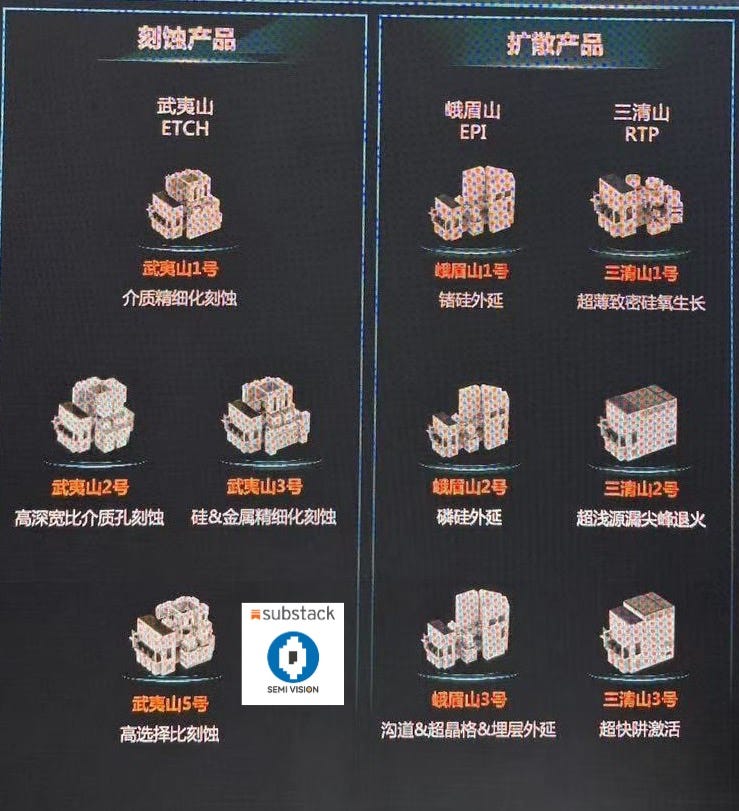

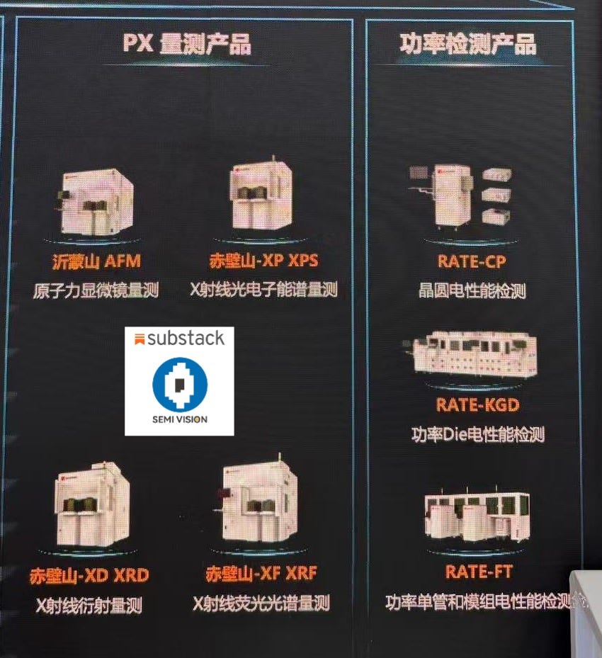
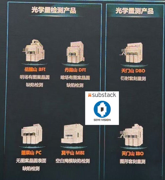
SiCarrier Core Equipment Highlights
EPI – “峨眉山” Series (Epitaxy)
• Tailored for third-generation semiconductor materials (SiC, GaN).
• Supports high-voltage chip fabrication ranging from 1200V to 6500V.
• Jointly verified with the Shenzhen Innovation Center for Third-Generation Semiconductors, focusing on automotive, industrial, and high-frequency power devices.
ETCH – “武夷山” Series (Etching)
• Equipped with proprietary electrostatic chuck (ESC) patent (CN119069414A) that enables 40% faster surface charge release, significantly improving yield.
• Aims to challenge the dominance of U.S.-based Lam Research in advanced etching technologies.
• Targets metal etching, high aspect ratio structures, and high-selectivity etch processes.
CVD – “長白山” Series (Chemical Vapor Deposition)
• Integrated with a patented reflective structure (CN119620268A); achieves 30% reduction in equipment footprintwhile improving deposition efficiency.
• Certified to ISO 9001, ensuring process reliability and quality consistency.
PVD – “普陀山” Series (Physical Vapor Deposition)
• Designed for 12-inch wafer compatibility, focused on advanced BEOL (Back-End-of-Line) metal interconnects.
• Achieves ±1.3 μm alignment accuracy, benchmarked against international leading PVD systems.
ALD – “阿里山” Series (Atomic Layer Deposition)
• Supports sub-7nm process nodes.
• Verified on SMIC Shenzhen’s production lines, ready for integration into advanced logic manufacturing.
SiCarrier Metrology & Inspection Strategy
Inspection
Focuses on defect detection after each process step – identifying contaminants, surface scratches, opens/shorts, etc.
Metrology
Delivers quantitative measurement of physical and material parameters such as film thickness, CD, etch depth, and surface morphology.
Metrology & inspection remains the least localized equipment category in China, and a key focus of U.S.-Japan export restrictions.
SiCarrier Breakthroughs in Metrology & Inspection
Three Competitive Advantages:
High Starting Point in Design
Built via forward engineering, targetingprecision, sensitivity, and WPH(wafers per hour) on par with global leaders.
In-House Development of Critical Components
Achieved domestic substitution of all core parts, ensuring supply chain security and technical independence.
Flexible Product Portfolio
Offers a range of high-, mid-, and entry-level tools, covering mainstream to leading-edge nodes (28nm to sub-7nm).
Representative Tools in Mass Production

The first XPS system has operated over 20,000 hours at a customer site, with all key metrics meeting advanced node production standards — validating product maturity and reliability.


PreviousNext
TopLatestDiscussions








See all